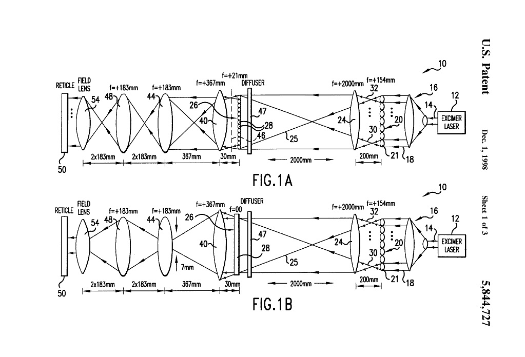
This invention relates to optics and, in particular, to an optical system for use in a scanner for processing semiconductor wafers.
BACKGROUND
In certain types of semiconductor wafer fabrication systems, a source of light illuminates a reticle (or mask), and the pattern on the reticle is then focused on the wafer surface to expose a layer of photoresist. In one type of exposure system, the illumination light is a relatively narrow strip of light which is then scanned across the reticle to expose the photoresist on the wafer.
State-of-the-art wafer fabrication systems also incorporate a step-and-repeat exposure system, where a pattern from a reticle is illuminated on only a portion of the wafer surface to expose the photoresist layer.
The wafer is then stepped with respect to the reticle pattern such that, ultimately, the entire wafer is exposed to the reticle pattern. A scanning exposure technique may be used in conjunction with such a step and-repeat type system.
As is well known, the illumination of the reticle in a scanning system must be uniform to obtain an accurate and predictable pattern on the wafer. That is, the light intensity incident on the reticle must ideally be the same at all positions along the reticle, perpendicular to the scanning direction, as well as exhibiting equal energy weighting versus incident angle. Such light characteristics ensure that all areas on the wafer will be identically exposed by the reticle pattern.
Various optical systems have been employed between the light source and the reticle in an attempt to obtain more uniform illumination. Due to non-uniformity in the light output by the light source, such as a laser, it is very difficult to obtain substantially uniform illumination of the reticle.
The present invention is an illumination design for a scanning microlithography system which provides a substantially uniform illumination of the reticle.
This invention relates to optics and, in particular, to an optical system for use ina scanner for processing semiconductor wafers.
BACKGROUND
In certain types of semiconductor wafer fabrication systems, a source of light illuminates a reticle (or mask), and the pattern on the reticle is then focused on the wafer surface to expose a layer of photoresist. In one type of exposure system, the illumination light is a relatively narrow strip of light which is then scanned across the reticle to expose the photoresist on the wafer.
State-of-the-art wafer fabrication systems also incorporate a step-and-repeat exposure system, where a pattern from a reticle is illuminated on only a portion of the wafer surface to expose the photoresist layer.
The wafer is then stepped with respect to the reticle pattern such that, ultimately, the entire wafer is exposed to the reticle pattern. A scanning exposure technique may be used in conjunction with such a step and-repeat type system.
As is well known, the illumination of the reticle in a scanning system must be uniform to obtain an accurate and predictable pattern on the wafer. That is, the light intensity incident on the reticle must ideally be the same at all positions along the reticle, perpendicular to the scanning direction, as well as exhibiting equal energy weighting versus incident angle. Such light characteristics ensure that all areas on the wafer will be identically exposed by the reticle pattern.
Various optical systems have been employed between the light source and the reticle in an attempt to obtain more uniform illumination. Due to non-uniformity in the light output by the light source, such as a laser, it is very difficult to obtain substantially uniform illumination of the reticle.
The present invention is an illumination design for a scanning microlithography system which provides a substantially uniform illumination of the reticle.