トライアルに挑戦しましたがダメでした。
別のトライアルに挑戦しました。またダメでした。
これを延々と続けてもおそらくプロにはなれません。
なぜダメだったのか、どこをどうすれば良かったのか、
トライアル受験後の分析がどこまでできていますか?
問題はそこです。
次のトライアルに活かせる気づきがあったでしょうか。
気づきを蓄積していくプロセスが確立されているでしょうか。
このプロセス確立がないまま、トライアルの数勝負だけを
延々と続けてもプロへの道は拓けてはきません。
おそらく20-30件ぐらいトライアル受験して
挫折してしまうのではないでしょうか。
トライアルは毎回内容が違います。
初見でどのように挑戦するのか。
内容の違うトライアルにも応用可能な訳出プロセスを確立しておく
必要があります。
この記事では、実際の特許を素材に、初見でどう切り込むのか、
初心者がどのようなアプローチをすれば、ノウハウ蓄積プロセスを
確立できるのか、という観点から、トライアル挑戦プロセスを
シミュレーションしてみたいと思います。
目次
トライアルとして選んだ特許
ここでは、以下の特許(部分)がトライアル課題文として、
出題されたと仮定して、初心者がどのように切り込んでいけばいいのかを
お見せしたいと思います。
いきなり下の解説を読まないで、
まずは自力でやれるところまでやってみてください。
FIELD OF THE INVENTION
This invention relates to optics and, in particular, to an optical system for use in a scanner for processing semiconductor wafers.
BACKGROUND
In certain types of semiconductor wafer fabrication systems, a source of light illuminates a reticle (or mask), and the pattern on the reticle is then focused on the wafer surface to expose a layer of photoresist. In one type of exposure system, the illumination light is a relatively narrow strip of light which is then scanned across the reticle to expose the photoresist on the wafer.
State-of-the-art wafer fabrication systems also incorporate a step-and-repeat exposure system, where a pattern from a reticle is illuminated on only a portion of the wafer surface to expose the photoresist layer.
The wafer is then stepped with respect to the reticle pattern such that, ultimately, the entire wafer is exposed to the reticle pattern. A scanning exposure technique may be used in conjunction with such a step and-repeat type system.
As is well known, the illumination of the reticle in a scanning system must be uniform to obtain an accurate and predictable pattern on the wafer. That is, the light intensity incident on the reticle must ideally be the same at all positions along the reticle, perpendicular to the scanning direction, as well as exhibiting equal energy weighting versus incident angle. Such light characteristics ensure that all areas on the wafer will be identically exposed by the reticle pattern.
Various optical systems have been employed between the light source and the reticle in an attempt to obtain more uniform illumination. Due to non-uniformity in the light output by the light source, such as a laser, it is very difficult to obtain substantially uniform illumination of the reticle.
The present invention is an illumination design for a scanning microlithography system which provides a substantially uniform illumination of the reticle.
トライアルの取り組み方
課題文の出典の有無の調査
まず、Googleを使って、第一文をフレーズ検索してみます。
フレーズ検索とは、” ”のようにダブルクォーテーション「”」で
キーワード又は言葉の並びを囲んで検索するものです。
実際にやってみましょう。
“This invention relates to optics and, in particular, to an optical system for use in a scanner for processing semiconductor wafers.”
Google検索の結果が出ました。
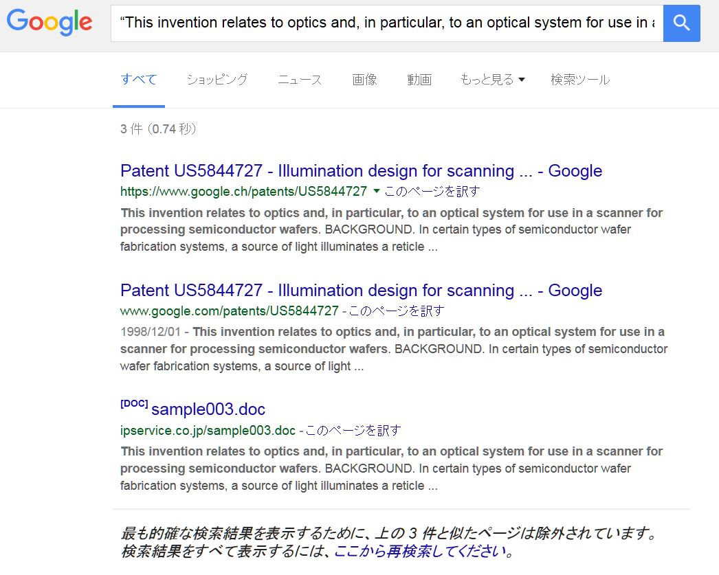
このトライアルの出典が、「US5844727」と判明しました。
該当特許からの情報取得
出典が判明したら、そこからできるだけ多くの情報を得るようにします。
まず、出願人が「Cymer, Inc.」、発明者が「William N. Partlo」
であることが分かります。
さらに、タイトルが
「Illumination design for scanning microlithography systems」
となっていること、及び、下図の中にある名称から見て、
リソグラフィー用の光学系であることが分かります。
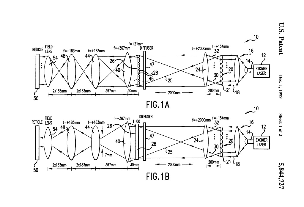
図から情報を読み取る練習をしてみましょう。
右端にある光源から出た光が、左端にあるレチクルに到達するまでの経路に
レンズが多数配置された光学系に関連する特許であることが分かります。
読みの正しさの確認
自分の読みが正しいかどうかを、本文中の該当箇所で確認してみます。
1A is a side view of one embodiment of the illumination system, assuming scanning is in a horizontal direction.
FIG. 1B is a top down view of the illumination system depicted in FIG. 1A.
上記記述から、自力で行った図からの情報の読み取りと、
特許の説明が合致していることが確認できました。
ちなみに、この時点で「リソグラフィー」「レチクル」「光源」「レンズ」
「エキシマレーザー」などのキーワードが理解できない場合、
何のことか全く分からない場合は、半導体関連の書籍を読む必要があります。
入門者向けの定評のある本を1冊読むことです。時間がなければ、
該当箇所(該当項目)だけの拾い読みで済ます場合もありますが、
できるだけ1冊は読み通してください。
これが無いと、問題となっている特許が果たす役割を、
その前後のプロセスとの関係で把握することができなくなり、
とんでも無い誤訳をしてしまう可能性があります。
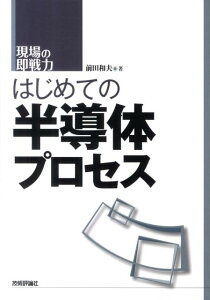
前田さんの本がオススメです。
これから料理をマスターしようとする人が、
「包丁」「なべ」「フライパン」がどういうものか、どうやって使うのか、
どういう機能を持っているか、が分からない状態であれば、
いきなり調理法を説明されても理解できないのと同じです。
横着しないで、当該分野において定番といえるような書籍は
必ず読むようにしてください。当業者の知識の常識部分は、
翻訳者も共有しておく必要があります。
ちなみに、トライアル課題文中、以下の赤でマークした部分は、
キーワード・キーフレーズです。
どのようなものか、どのような機能を持つのかが即答できないようであれば、
完全な知識不足です。これらを完全理解した後で無ければ、
トライアルの土俵に立つことはできないと考えてください。
FIELD OF THE INVENTION
This invention relates to optics and, in particular, to an optical system for use in a scanner for processing semiconductor wafers.
BACKGROUND
In certain types of semiconductor wafer fabrication systems, a source of light illuminates a reticle (or mask), and the pattern on the reticle is then focused on the wafer surface to expose a layer of photoresist. In one type of exposure system, the illumination light is a relatively narrow strip of light which is then scanned across the reticle to expose the photoresist on the wafer.
State-of-the-art wafer fabrication systems also incorporate a step-and-repeat exposure system, where a pattern from a reticle is illuminated on only a portion of the wafer surface to expose the photoresist layer.
The wafer is then stepped with respect to the reticle pattern such that, ultimately, the entire wafer is exposed to the reticle pattern. A scanning exposure technique may be used in conjunction with such a step and-repeat type system.
As is well known, the illumination of the reticle in a scanning system must be uniform to obtain an accurate and predictable pattern on the wafer. That is, the light intensity incident on the reticle must ideally be the same at all positions along the reticle, perpendicular to the scanning direction, as well as exhibiting equal energy weighting versus incident angle. Such light characteristics ensure that all areas on the wafer will be identically exposed by the reticle pattern.
Various optical systems have been employed between the light source and the reticle in an attempt to obtain more uniform illumination. Due to non-uniformity in the light output by the light source, such as a laser, it is very difficult to obtain substantially uniform illumination of the reticle.
The present invention is an illumination design for a scanning microlithography system which provides a substantially uniform illumination of the reticle.
日本の特許庁のデータベースでの調査
次に、日本の特許庁のデータベースを使って、関連特許の有無をチェックします。
これをやらないで、いきなり翻訳作業を開始する人がいますが、
絶対にやってはいけません。
例えば、トライアルの期限が10日後であれば、
1週間は関連特許・関連記述・キーとなる技術等の調査と理解に費やすべきです。
特許の一部を翻訳する「部分訳」のトライアルであっても、
必ず全文を翻訳してから該当箇所の訳文を提出して下さい。
このやり方をすることで、原文のミスが見つかることもありますし、
通常はこう訳すけれどもこの特許ではこう訳すべき、といった
特殊事情が見えてくることもあります。
特許情報プラットフォームにアクセスしたら、キーワードを選定して
数十件程度(該当特許を2日程度でざっと読める程度の件数)
まで絞り込みます。
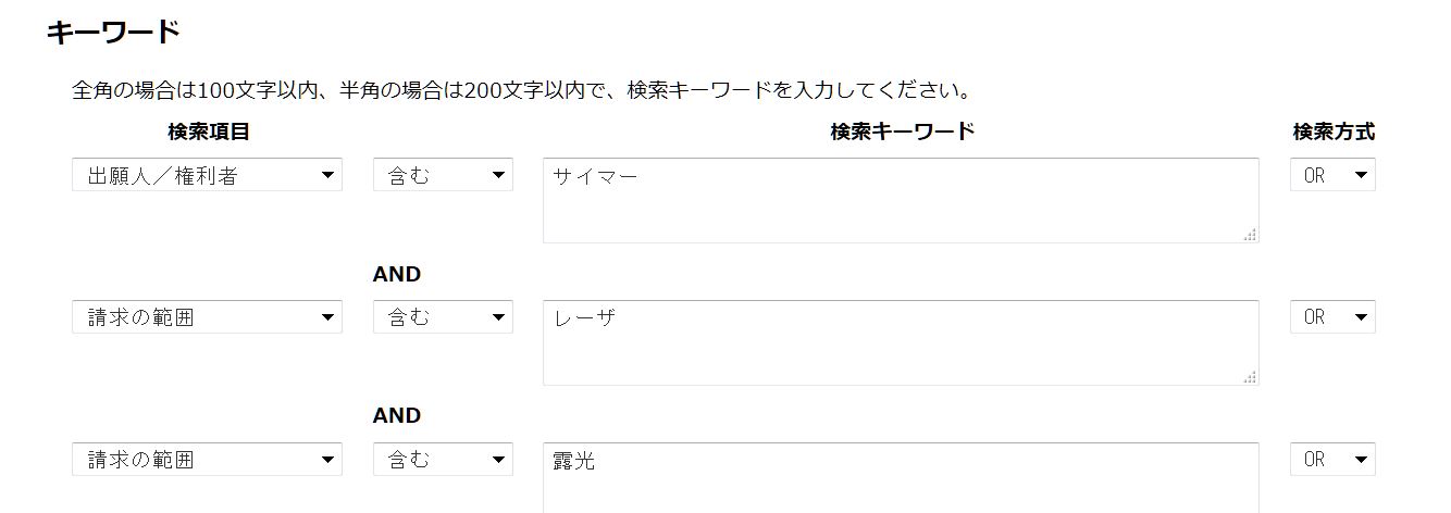
この検索条件で、

という結果です。
どの項目に、どのようなキーワードを入れて、
何件ぐらいで検索作業を収束させるかは、
何度もやってみてコツを掴む必要があります。
この作業がいきなりできるものではありませんので、
試行錯誤して身につける必要があります。
ここでは件数が9件ですから、それらすべてを読んで、
トライアルの出典となった特許と似た図面が含まれないかどうかを
調べることができます。
また、出願人が特許で使っている言葉使い等になれるためにも、
できるだけ多くの明細書に目を通したほうが有利です。
対訳の有無を調査
DJSOFTのE’Storage2016を使って、
出典に使われた英文特許に日本語訳が存在しないかを調査します。
そうすると、以下の日本語訳が存在することが分かりました。
【発行国】日本国特許庁(JP)
【公報種別】公表特許公報(A)
【公表番号】特表2001-515268(P2001-515268A)
【公表日】平成13年9月18日(2001.9.18)
【発明の名称】走査式マイクロ・リソグラフィー・システム用の照明設計
では、この公開訳文中から該当箇所をそのまま解答として使っていいのでしょうか?
対訳が存在する場合の注意点
出題者側が、対訳が存在する特許をトライアル課題文の素材として
敢えて使った意図、すなわち「出題意図」を読む必要があります。
初心者は、対訳がないかな?→検索→あった!→やった→このまま使おう
というふうに考えがちですが、過去見てきた類似のケースからみても、
この場合は、出題者が公開訳文に対して「不満」がある場合がほとんどです。
出題者は、あなたがその訳文を「バージョンアップ」できますか?
と問うていることになります。これが出題意図です。
だから、公開訳文から該当箇所をそのまま抜き取って回答した段階で、
速攻NGだと思ってください。
なので、あえて周辺部から攻めて、一見遠回りするような作業を
しているわけです。
訳文から入ると、どうしてもそれに引きずられてしまいます。
誤訳を引きずって訳文を作成すると、
やはり不満足な訳文になってしまう可能性があるのです。
今回はたまたま対訳が存在しました。
しかし、対訳が存在すれば対応できるけれど、
対訳が無い場合には、手も足も出ないということでは困ります。
対訳の有無に関係なく、トライアルに対応できるように、
普段から対応スキームを模索し、確立しておく必要があります。
まとめ
このようにトライアルの出典として使われた特許に対訳が存在する場合には、
より一層慎重な対応が求められます。
当該対訳だけでなく、同一出願人、同一発明者の特許を複数確認して、
用語の選択、言葉の運び等を分析して下さい。
トライアルを受けられる際には、調査・知識獲得8割、訳出1割、確認1割
ぐらいの時間配分がお勧めですが、対訳の有無に関わりなく対応できるように
様々なアプローチをぜひ用意しておいて下さい。

「レバレッジ特許翻訳講座では、
どのような講義をやっているのか見てみたい」
という声にお応えして、「講座の動画32本」を無料でプレゼントする
キャンペーンを行っていますので、ぜひ下記フォームからご利用下さい。
(必須事項はピンクのところだけで、あとは任意ですので
差し支えない範囲でご記入下さい)
動画プレゼント
受講感想を原文のまま「卒業生の声」として
HPに一部掲載していますのでぜひ読んでみて下さい。
より多くの卒業生の声は、
こちらの「資料請求」から入手できる「講座案内」に
掲載されていますので、よろしければご利用下さい。